From thermal challenges to a controlled light source
How a difficult stray-light challenge became a family of visible and near-infrared optical systems
Company: Imatest LLC
Role: Mechanical Engineer and product-development lead
Scope: Project leadership, optomechanical architecture, thermal development, precision alignment, SolidWorks CAD, prototyping, testing, electrical integration, suppliers, documentation, and production release
Outcome: Multiple generations and wavelengths of a released LED source integrated into Imatest’s camera stray-light testing system
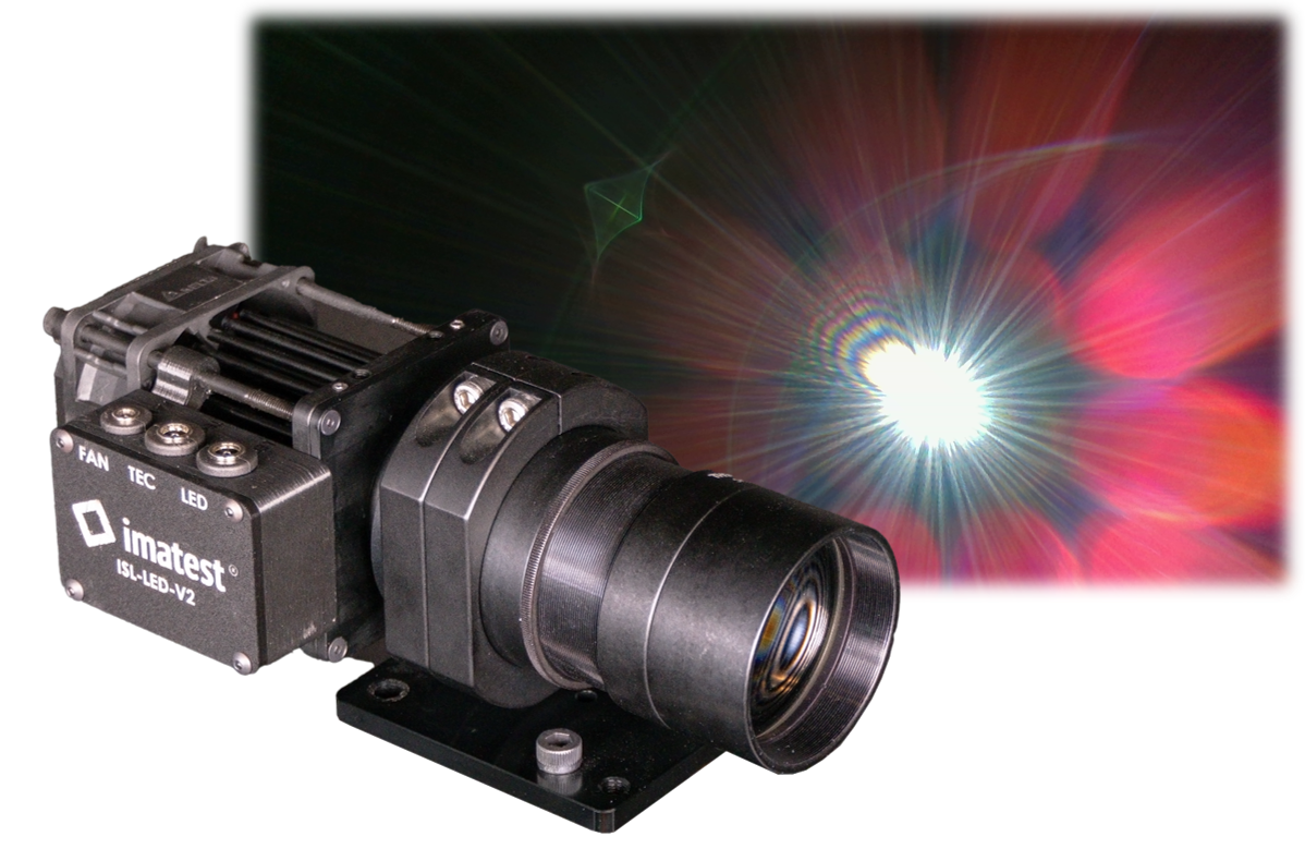
Why the product mattered
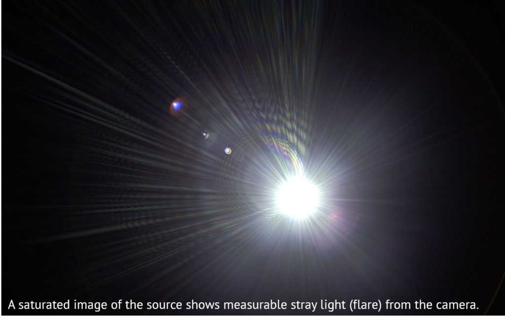
Stray light, also known as flare, is light that reaches a camera sensor through something other than the intended optical path.
It can create ghost objects, wash out contrast, obscure real scene information, and reduce the usable dynamic range of the camera. Those effects are undesirable in any image, but they become especially important when automotive, machine-vision, security, and other computer-vision systems rely on camera data to interpret their surroundings.
Consider a vehicle camera facing a low sun. The imaging system must distinguish real objects from optical artifacts and retain useful scene information despite an intense light source near or inside its field of view.
Manufacturers need a repeatable way to reproduce those conditions, measure the resulting flare, and understand how the camera responds. That requires a small, extremely bright, carefully controlled light source, not simply a powerful lamp.
When the first approach did not solve the problem
Imatest initially engaged an outside company with relevant lighting expertise to develop the source. I worked with that team throughout the process, helping communicate and evaluate our optical, mechanical, usability, and commercial requirements.
The delivered prototype demonstrated how difficult the problem really was. It was considerably larger and more expensive than a viable customer product could be, difficult to position within the test system, underpowered for the application, and unable to meet several established performance requirements.
It could not be refined into the product we needed, and no one was taking ownership of restarting the effort. I stepped in and led a new internal approach.
An image scientist worked closely with me throughout the project. He brought deep knowledge of image science and performed the camera-based evaluation. I drove the development process, mechanical architecture, physical experimentation, and integration of the complete product.
When we encountered optical behavior beyond our combined expertise, we found and hired an optical specialist. Recognizing when the team needed deeper expertise was part of leading the project responsibly.
Beginning with a practical first generation
The first generation used an off-the-shelf commercial LED source.
It did not provide the brightness or performance we ultimately wanted, but it gave us a practical starting point. It allowed us to develop the wider test system, understand the optical behavior, validate customer needs, and learn what a purpose-built source would have to accomplish.
That first version reduced the number of unknowns before we attempted the much harder second-generation design.
The halo problem
One of the most difficult requirements was suppressing the halo created by the light source itself.
The purpose of the product was to reveal stray light generated by the camera under test. If the source introduced a large optical halo of its own, that unwanted light contaminated the captured image and undermined the measurement.
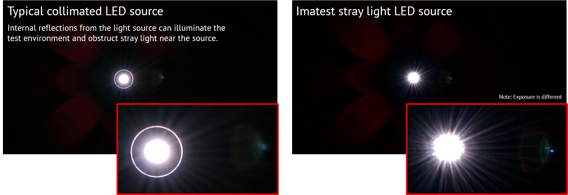
Solving the problem required careful control of the light entering the collimating optics. The source, PCB, mechanical interfaces, and optical components needed a precise alignment strategy that could be adjusted during assembly and then retained through use.
Small errors could compromise the beam. This made the PCB and its mounting architecture part of the precision optomechanical system, not simply an electrical component placed inside an enclosure.
Designing the second generation
I led the development of the second-generation source around a custom, overdriven single-LED architecture.
Compared with the first generation, the new design pursued greater brightness, a smaller apparent source, improved beam behavior, better integration, and a more practical product package.
The work combined:
- A custom aluminum-core LED PCB
- Thermoelectric cooling
- Heat sinking and forced airflow
- Precision optomechanical alignment
- Adjustable source positioning
- Optical and thermal experimentation
- Connectors, power supplies, and driver electronics
- A dedicated electrical integration box
- Mechanical packaging for mounting and service
The second generation was not one product. I developed the visible-light version and two near-infrared versions for different testing needs.
Solving one problem created another
The optical requirements placed severe constraints on the thermal design.
Only one LED could be used, but it needed to produce far more intensity than an ordinary lighting application. The optical architecture also restricted airflow around the source, exactly where heat most needed to be removed.
The second-generation product therefore depended on the complete thermal path:
- An aluminum-core LED PCB
- Carefully controlled thermal interfaces
- A thermoelectric cooler
- Heat sinking
- Forced airflow
- Driver and power electronics
- The mechanical structure connecting those elements
I used thermocouples extensively during development to understand the real thermal behavior. We considered adding closed-loop temperature sensing to the final product, but the packaging and system complexity made an integrated sensor impractical.
Instead of implying the desired feedback loop existed, the final design had to achieve acceptable thermal performance through the physical architecture and selected operating conditions.
The painful details between a concept and a product
Many of the hardest lessons came from interfaces that looked simple on paper.
Thermal-interface materials did not perform as consistently as idealized calculations suggested. Small variations in thermal-paste application could change system behavior completely. Soldering to an aluminum-core PCB introduced manufacturing challenges that differed from the conventional boards we were accustomed to using.
The adjustable PCB mounting system needed enough movement to align the optical path without becoming unstable, difficult to assemble, or impossible to manufacture consistently. Tight tolerances could help one interface while making another harder to build.
Mechanical changes affected optical alignment. Optical constraints restricted cooling. Thermal solutions changed packaging, wiring, assembly access, and overall size. Connector selection, power supplies, and the electrical integration box added another group of interfaces that had to work within the same system.
This was not a project where each discipline could solve an isolated part and hand it over. The product worked only when the interfaces worked together.
Aligning light I could not see
Near-infrared development introduced a new challenge: the system still required precise optical alignment, and the beam had to be focused, but I could not rely on seeing the beam directly.
I designed assembly and alignment test fixtures that allowed us to position and validate the near-infrared sources through a controlled process rather than relying on visual judgment.
These fixtures turned an invisible and highly sensitive alignment problem into something technicians could perform and verify more repeatably.
The NIR work reinforced a lesson that appears throughout my engineering: when a process depends too heavily on individual intuition, the answer is often a better fixture, test, or feedback method.
Building, measuring, and refining
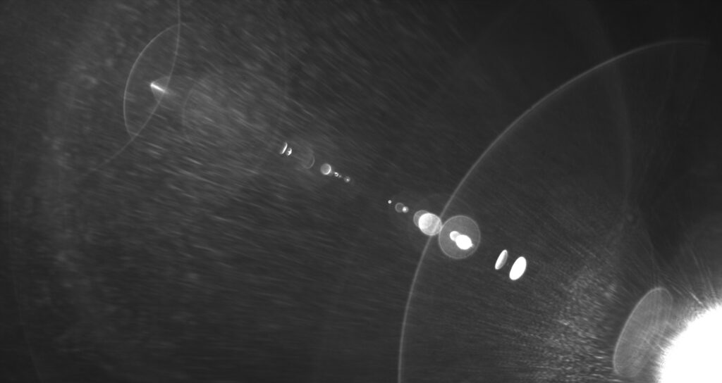
We worked iteratively: build a prototype, operate it under realistic conditions, capture images, measure temperature and optical behavior, identify the limiting mechanism, and revise the system.
The image scientist’s testing showed whether the source produced the camera response needed for meaningful stray-light analysis. Thermocouple measurements showed whether the LED and cooling system could maintain acceptable performance. Assembly exposed tolerance, alignment, soldering, thermal-interface, and packaging problems that were not visible in CAD.
There were many failed ideas, painful discoveries, and time-consuming roadblocks. I was the only mechanical engineer leading a product that crossed optics, thermodynamics, electronics, manufacturing, and image science. I did not always have the knowledge or tools I wished I had, but I kept learning, asked for help when the project needed it, and used the evidence from each failure to make the next version better.
That cycle gradually transformed a difficult optical experiment into a family of products that could be assembled, aligned, mounted, powered, operated, and supported.
The result
The work produced the original Imatest Stray Light LED Source and the second-generation visible and near-infrared sources.
The V2 source became part of a broader testing system that combined the source, camera-positioning hardware, controlled test conditions, and Imatest’s analysis software.
Together, these tools provided a practical way to project a small, intense source for characterizing flare, ghosting, veiling glare, diffraction effects, and other stray-light behavior across different incident angles.
What I would do differently now
I am proud of what I built, but I would not design the product the same way today.
Knowing what I know now, I would simplify parts of the architecture, address alignment and manufacturability earlier, bring specialized optical expertise into the process sooner, and create more deliberate validation steps before committing to later design decisions.
That is not a rejection of the work. It is evidence of how much the work taught me.
At each stage, I made the best decisions I could with the knowledge, tools, evidence, and resources available. Some decisions worked. Others led directly into another obstacle. I stayed accountable for both.
Good engineering is not pretending every decision was obvious in hindsight. It is learning fast enough to keep moving, being honest when an approach is not working, and carrying those lessons into the next product.
What the project demonstrates
This project did not turn me into a career optical scientist or thermal specialist. It taught me how to lead responsibly when a product refuses to remain inside one discipline.
I took ownership when the project lacked a driver. I learned enough optics, thermodynamics, electronics, and manufacturing to make informed decisions. I recognized when experimentation was more valuable than another assumption and when the team needed outside expertise.
Most importantly, I connected those disciplines and carried multiple generations of the product through development and release.
That is the kind of engineering challenge I like: a real problem that demands curiosity, persistence, humility, and the willingness to learn whatever the product needs.
Product information and images are provided by Imatest. This case study describes my engineering contributions to multiple generations of the Stray Light LED Source while employed as a Mechanical Engineer at Imatest LLC.